Z-Core: Performance Analysis
Benchmarking Z-Core — DOOM FPS across cache configurations, then CoreMark/MHz, STREAM and pointer-chase results.
A RISC-V RV32IM_Zicsr soft core designed from first principles in synthesisable Verilog. This deep dive walks through the microarchitecture stage by stage, then analyses its measured performance on FPGA.
Z-Core is a RISC-V RV32IM_Zicsr processor I designed from scratch in synthesisable Verilog, and then grew into a full system-on-chip around it. It implements the 32-bit base integer ISA (RV32I), the M extension for hardware multiply and divide, and the Zicsr extension for the control-and-status registers that back machine-mode trap handling and the hardware performance counters. Surrounding the core sits an AXI4-Lite interconnect wiring up main memory and a handful of peripherals: UART, GPIO, a 64-bit timer and, on the FPGA build, a VGA controller.
The aim was never just to get it running, but to get it running well, and to understand exactly where every cycle goes. That meant balancing a classic in-order pipeline, building the forwarding and stall logic that keeps it fed, adding a branch predictor to hide control-flow penalties, and designing a memory hierarchy capable of achieving single cycle throughput for memory operations. This is demonstrated by a deep performance analysis presented in the Z-Core performance deep-dive post, where Z-Core ends up running DOOM at playable framerates, and reporting performance metrics compared to state-of-the-art processors for embedded applications. This page is the other half of the story: how the microarchitecture is actually built, stage by stage.
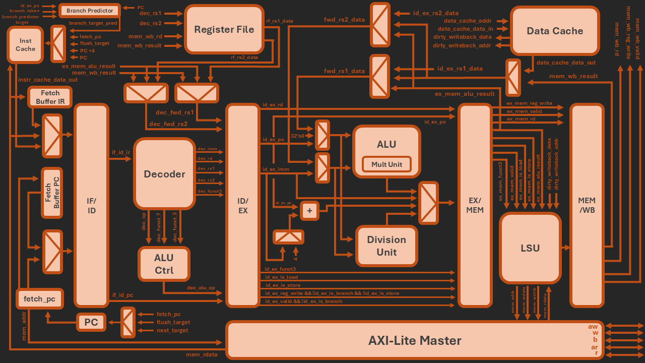
Top-level datapath: the 5-stage pipeline (IF/ID → ID/EX → EX/MEM → MEM/WB) with the register file, decoder, ALU and multiplier, division unit and LSU, the split instruction/data caches, the branch predictor and the AXI-Lite master, plus the inter-stage forwarding paths.
The pipeline follows the textbook five-stage layout: IF (instruction fetch), ID (decode & register read), EX (execute / ALU / branch resolution), MEM (data-memory access) and WB (register write-back), separated by pipeline registers.
Branches and jumps are the natural enemy of any pipeline, so Z-Core hides them behind a 2-bit dynamic branch predictor. It pairs a Branch History Table (BHT), holding the 2-bit saturating counters that say strongly taken / weakly taken / weakly not-taken / strongly not-taken, with a Branch Target Buffer (BTB) caching the destination address. Both are direct-mapped and indexed by the PC. The fetch stage can therefore speculate down the predicted path without waiting for the branch to resolve. Once the prediction is done, both the predicted direction and the target are forwareded through the pipeline until the actual condition is evaluated in EX stage. On a misprediction the pipeline is flushed and redirected to the correct program counter. If the correct target is already sitting in the instruction cache, that flush costs just a single cycle, stretching to ~12 only on the rare occasion the re-fetch also misses the cache.
Data hazards are resolved by a forwarding unit that bypasses results from the EX/MEM and MEM/WB pipeline registers back into the EX inputs, eliminating stalls for back-to-back dependent ALU instructions. The one case forwarding cannot cover is a load-use hazard, where an instruction needs a value still in flight from memory. This is caught by the hazard-detection unit, which inserts a single bubble into the pipeline.
The M extension splits into two very different units, because multiply
and divide have very different costs in hardware. Multiply lives inside
the ALU as a single-cycle, fully combinational 32×32→64-bit unit: the
synthesis-friendly version is written around the Verilog * operator so the
tool maps it straight onto the MAX 10's embedded 18×18 multipliers. (A second, structural Patterson & Hennessy partial-product
tree multiplier is kept in the repo alongside it, it produces same result, but built from a
binary tree of 32-bit adders for when I wanted to see the textbook architecture in RTL
rather than let the tool infer it.)
Divide is the expensive one. It is a separate iterative
restoring divider (the shift-subtract-restore algorithm from Patterson &
Hennessy) covering DIV/DIVU/REM/REMU,
and it cannot finish in a single cycle. When a division reaches EX it raises a
div_running signal that stalls the front of the pipeline (freezing the PC,
IF/ID and ID/EX registers) for the ~68 cycles the iteration takes, then
releases the stall and lets the quotient or remainder flow on to MEM and WB. Operands are
forwarded into the divider from the MEM and WB stages exactly like any other ALU input,
so a divide never sees stale data.
Everything outside the core (main memory and every peripheral) hangs off a single AXI4-Lite bus through an interconnect that decodes the address map and routes each access to the right slave. The core drives that bus with one AXI master shared between instruction fetch and data access, behind a small arbiter that gives load/store priority over fetch when both want the bus in the same cycle. It is clean and standard, but it is also slow: a single AXI round-trip to main memory costs on the order of 10–11 cycles. If we always fetch from main memory, the bus would make the five-stage pipeline spends almost all of its time waiting, this is precisely the bottleneck that made early DOOM unplayable at under one frame per second.
The fix is a split L1 cache, one cache per side of the pipeline, both designed for single-cycle throughout, so a cached access looks no different from an ALU op:
request_refill and
hands the LSU a writeback address and victim line in case the evicted line is dirty. Then the
LSU performs the AXI writeback, fetches the missing line, and installs it. On the FPGA
build it is 32 KB.
Both caches synthesise to the MAX 10's M9K blocks, and together they are the biggest performance lever in the whole design. The jump from no cache to I-cache + D-cache is what turns Z-Core from a curiosity into something that runs DOOM and performs hand-by-hand with comercial processors. The performance deep-dive takes that apart cycle by cycle, including a deep dive into the pipeline and analytical model performance comparison.
The Zicsr extension adds the six CSR instructions
(CSRRW/S/C and their immediate variants), each an atomic read-modify-write:
the old value lands in rd while the new value is written in the same EX
cycle, with the spec's write-suppression rules for the x0/zero-immediate
cases. Those instructions sit on top of a machine-mode CSR file
(mstatus, mtvec, mepc, mcause,
mtval, mie/mip, mscratch) implementing
a subset of the M-mode privileged architecture (Privileged Spec v1.12).
Z-Core is M-mode only, enough for bare-metal embedded code without the complexity of full
privilege levels.
The same trap logic handles both synchronous exceptions (illegal
instruction, ECALL, EBREAK, and misaligned load / store /
instruction-fetch addresses) and asynchronous interrupts (external,
software and timer, prioritised external > software > timer). On a
trap the hardware does it all in one cycle: latch mepc (the faulting PC for
exceptions, the next instruction for interrupts), record the cause in mcause
and any faulting instruction/address in mtval, save the interrupt-enable bit
(MPIE ← MIE, then MIE ← 0), redirect the PC to
mtvec in direct mode, and flush the in-flight instructions just like a
mispredicted branch. MRET reverses it: MIE ← MPIE,
MPIE ← 1, and the PC returns to mepc. One small but
important detail: an all-zeros instruction word is treated as a NOP rather
than an illegal instruction, so executing uninitialised memory never spirals into an
infinite trap loop.
The CSR file also carries the performance counters that made the
benchmarking work possible: the standard mcycle and minstret,
plus eight custom mhpmcounters wired to events I actually cared about:
instruction- and data-cache hits and misses, load and store counts, branch
mispredictions and pipeline flushes. Being able to read those straight out of the running
core is what let me attribute cycles precisely in the performance analysis.
Z-Core was characterised in two dimensions:
timing and area from FPGA synthesis, and real throughput from running benchmarks on the
board. The hardware was built with Intel Quartus Prime Lite for the
MAX 10 10M50DAF484C7G on the Terasic DE10-Lite, clocked at
50 MHz; software was cross-compiled with the RISC-V GNU toolchain
(-march=rv32im_zicsr, -mabi=ilp32, -O2) and loaded
over a UART bootloader. On the benchmark side I ran CoreMark for a
portable, comparable score, STREAM for sustained memory bandwidth, a
pointer-chase microbenchmark for raw memory latency, and (because it is
a far more honest stress test than any synthetic loop) DOOM, measured in
frames per second across cache configurations. The full performance analysis, with charts and the
analytical model behind every number, is in the
performance deep-dive post.
On the area side, the two 32 KB caches, and the 16KB BRAM for the bootloader dominate the on-chip memory budget (they infer the MAX 10's M9K block RAM rather than logic blocks), while the M-extension multiplier maps onto the device's embedded 18×18 multipliers instead of being built out of logic elements.
Verification happened at two levels. A large self-checking system-level
testbench drives the whole SoC through a directed regression suite: over
300 checks spanning arithmetic, logic and shifts, loads/stores down to
byte and halfword granularity, branches and jumps, RAW-hazard and forwarding stress,
the M-extension, CSR read/modify/write, exceptions and timer interrupts (including the
nasty corners: an IRQ landing mid-prediction, an exception at a mispredicted branch
target, MRET returning into a predicted loop), and dedicated I-cache and
D-cache stress (locality loops, conflict-miss thrash, dirty-writeback persistence, way
conflicts). Underneath it, each block (ALU, decoder, register file, multiplier, divider,
both caches, and the branch predictor) has its own dedicated unit testbench. The verification process
was supported by AI-assisted tools, which I believe can be genuinely valuable for verification,
helping to ease the burden of exhaustive testing and accelerating the design process.
Directed tests prove the cases I thought to write; for everything else, Z-Core is run
through the official RISCOF architectural compliance flow, which
cross-checks the core's committed register and memory state against a golden ISA reference
model. It passes all 109 tests (48 RV32I, 45 RV32M and 16 Zicsr) at a
100% pass rate, including the misalign and ebreak suites.
Still, this verification is not yet at industry sign-off standard. A more thorough process would be needed before I would send the processor to tapeout.
Source code, testbenches and the FPGA project are on GitHub: the Z-Core core ↗ and the Z-Core-FPGA implementation ↗.